
Advanced Nano Electronics Laboratory
: The Team - Choi Research Lab.
We are studying on the engineering of thin film materials and processes for emergent electronic applications.

Advanced Nano Electronics Laboratory
: The Team - Choi Research Lab.
We are studying on the engineering of thin film materials and processes for emergent electronic applications.

To enable unique nanoelectronic applications;
1) The design and synthesis of engineered thin film for specific functions are required. Composites, nanolamellar or randomly mixed heterogeneous materials can create artificial materials with novel properties to overcome the limitation of conventional CMOS technology. New computing memory and transistor for the next generation are under investigation.
2) Atomic layer deposition (ALD) process has an advantage for very thin and conformal film growth. ALD process including surface treatments can modify the hydrophobic surface of low-dimensional nanomaterials for the fluent nucleation of the films. Additionally, ALD-grown film can act as a good gas barrier and provide extremely enhanced mechanical properties. Film growth behaviors and electrical/chemical/mechanical/optical properties of ALD-coated nanomaterials can be characterized. Inter-laboratory, inter-university, and interdisciplinary research and collaborations are on going now.
If you are interested in those researches and activities, please come and join us and do make it matter!
News
+-
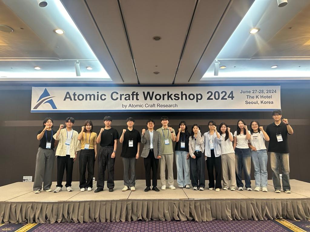
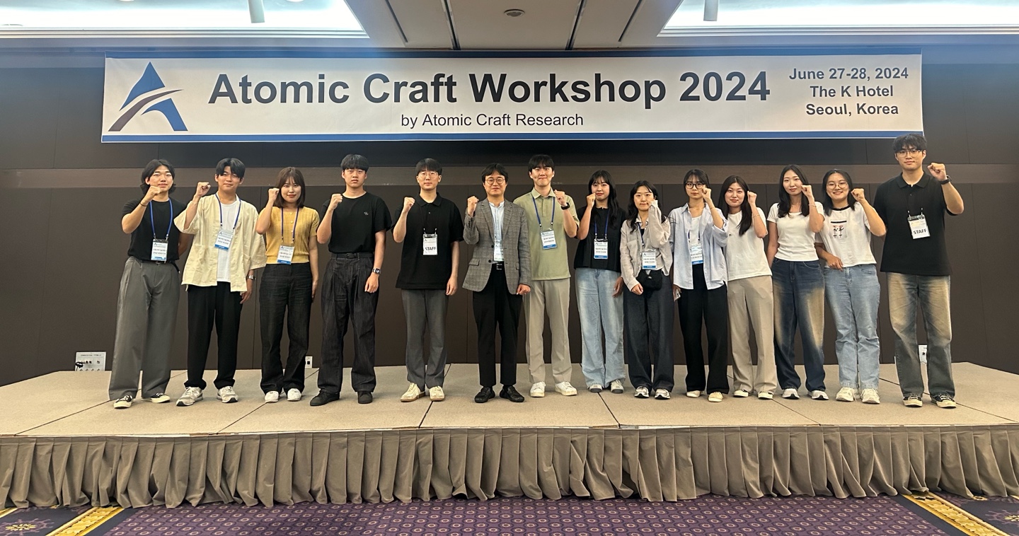
June 27-28, 2024 2024.07.01 - 2024 Atomic Craft Workshop
-
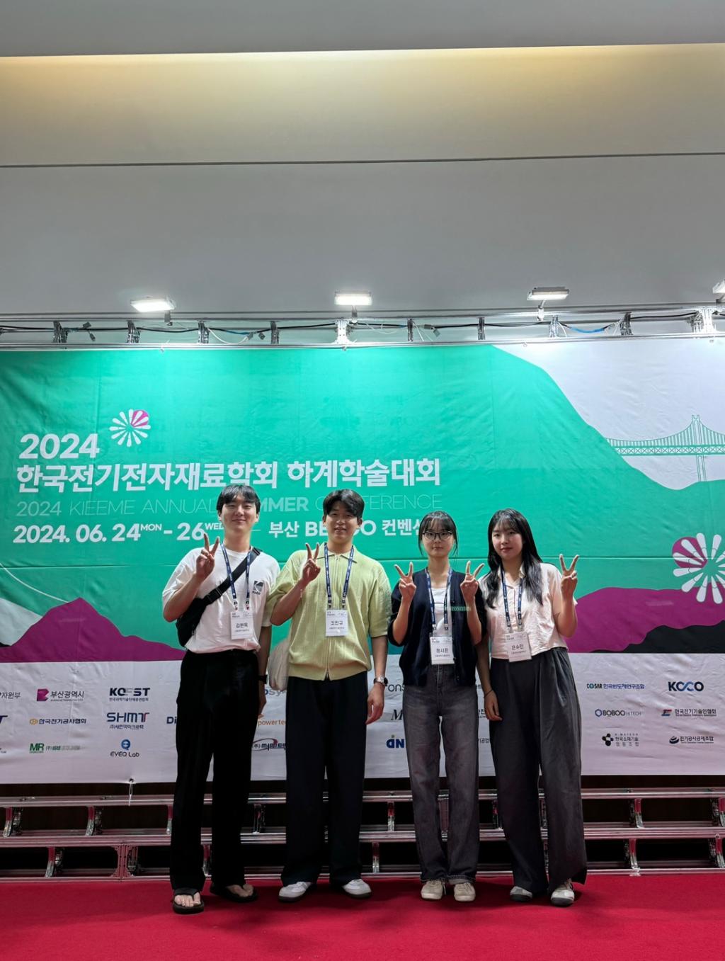
June 24-26, 2024 2024.07.01 - 2024 한국전기전자재료학회 하계학술대회
-
March 28-29, 2024 2024.04.03 - KPMI(한국분말재료학회) 2024 춘계학술대회
-
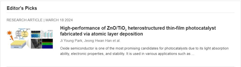
논문 출판 2024.03.20 박지영 학생의 논문 "High-performance of ZnO/TiO2 heterostructured thin-film photocatalyst fabricated via atomic layer deposition"이 저널 Editor's Picks에 선정되어 출판되었습니다.